Research
CRISP’s basic research aim is to discover and develop novel materials that have been engineered at the scale of individual atoms. To this end, CRISP has two interdisciplinary research groups (IRGs) that focus on: (1) characterizing, designing, and controlling the novel chemical, electronic, and magnetic properties that arise at complex oxide interfaces, and (2) developing new bulk metallic glasses and advancing the fundamental understanding of their behavior which in turn will enable surface property engineering through multi-scale patterning. The research in the two IRGs will advance a wide range of technologies spanning computation, communication, energy, and medical applications.
Below there is a brief description of the research aims of the two IRGs.
IRG1: Transferring electrons to a superconductor
IRG1: Teaching neural networks via materials science
IRG1: Tailoring Topological Surface States
IRG1: New Haven Science Fair Participation
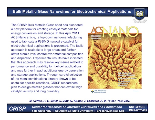
IRG2: Combinatorial Screening of Metallic Glass Electrocatalysts for the Oxygen Reduction Reaction
IRG2: Developing a Solar Outreach Program for Haiti
IRG2: Nanoscale Effects on Critical Cooling Rates of Metallic Glasses
Public Talk Series: Science Saturday: “Watching Atoms Move”
Seed: Clearing the Way for Quantum Information
Empowering the Next Generation of Female and Minority Scientists in STEM
Education and outreach: Mysteries of Sand! CRISP Public Lecture
Education and outreach: Math & Science in the Elementary School Classroom
National Collaboration: MBE System at the National Synchrotron Light Source II
MBE System for Undergraduate Teaching
IRG1: Transferring electrons to a superconductor
IRG1: Teaching neural networks via materials science
IRG1: Tailoring Topological Surface States
IRG1: New Haven Science Fair Participation
IRG2: Combinatorial Screening of Metallic Glass Electrocatalysts for the Oxygen Reduction Reaction
IRG2: Developing a Solar Outreach Program for Haiti
IRG2: Nanoscale Effects on Critical Cooling Rates of Metallic Glasses
Public Talk Series: Science Saturday: “Watching Atoms Move”
Seed: Clearing the Way for Quantum Information
Empowering the Next Generation of Female and Minority Scientists in STEM
Education and outreach: Mysteries of Sand! CRISP Public Lecture
Education and outreach: Math & Science in the Elementary School Classroom
National Collaboration: MBE System at the National Synchrotron Light Source II
MBE System for Undergraduate Teaching
 The atomic structure along step edges on metal oxide surfaces is crucial for the growth of overlayers in complex oxide devices. No experimental techniques are yet capable of resolving that structure. Ab initio calculations of step structures on metal oxides are complex and have not been reported to date.
By taking into account both the ionic and covalent components of interatomic bonding in metal oxides, we have developed a method of predicting the relative stability of different step structures. Fe3O4 (magnetite) is a ferrimagnetic metal that is of interest for spintronics applications and as a substrate for growing complex oxides. STM observations on Fe3O4 (100) surfaces show alternating smooth and jagged step structures. By evaluating the coordinative unsaturation of step-edge ions and the excess charge along a step, we find that steps having the smallest excess charge will be most stable. The most probable arrangement of cations and anions along the step edges can be predicted.
 |
 |
| Stable step structure (a-type) | Unstable step structure (b-type) |
 CRISP collaborates with leading chip maker Advanced Micro Devices (AMD) to develop new gate insulator materials for next generation processors.
Further miniaturization of transistors for use in processors and memory applications necessitates the replacement of the traditional SiO2 gate insulator in these devices with so-called high-k materials. These materials can greatly reduce unwanted leakage currents in transistors. Candidate materials include complex oxide materials, such as strontium titanate (SrTiO3). Yale has the capability to deposit single crystalline strontium titanate directly onto silicon wafers.
 |
 |
| Fig.1 Atomic resolution transmission electron microscopy (TEM) image of epitaxial SrTiO3 on Si. | Fig.2 Custom-built oxide molecular beam epitaxy (MBE) system at Yale. |
The ability to grow materials layer by layer with atomic precision opens the door to control and engineering of materials properties. During the growth of SrTiO3, we can insert a pair of atomic layers of LaAlO3 as shown at left. Our first principles theory shows that the polar nature of inserted LaO and AlO2 layers causes a shift between electronic band energies of the SrTiO3 on the two sides. Repeated insertions of such layers should allow experimenters to create larger accumulated shifts as well as quantum wells that can trap electrons for further control over their properties
Band energy shift delta V at various levels of theory:
- Bare LaO /AlO2- charged sheets : 24 eV
- Electronic screening of SrTiO3 : 4.5 eV
- Ionic electronic screening : 0.5 eV
 |
| SrTiO3-LaAlO3-SrTiO3 layer system 0.5 eV from first principles |
Nanoscale metallic structures are promising platforms for sensors: using photons to launch surface plasmon polaritons, metallic nanowires can guide and re-emit light over tens of microns. The re-emission of light at the other end of a nanowire can be promoted or altered by adsorption of molecules.
Using silver nanowires synthesized in solution and fabricated by electron-beam lithography, we observe plasmons as re-emitted light after laser stimulation at different frequencies and polarizations (1, 2), or at multiple points using Holographic Optical Tweezers (3). By controlling the size, geometry and orientation of the nanoparticles and the frequency, polarization and angle of the incoming light that creates the plasmons, we aim at building a platform for sensing molecules.
 |
|
 |
 |
| Synthesized Ag wires (830 nm laser) | Synthesized Ag wires (1064 nm laser) |
Almost all electronic devices currently in use involve thin films of one material in contact with another material. The proper operation of a device depends strongly on the properties of the interfaces between the thin films.
By using electron spectroscopic techniques that can see several layers of atoms into a solid, we have been able to identify electronic states that exist only at the interface between the ferrimagnetic oxide Fe3O4 (the mineral magnetite) and antiferromagnetic CoO. Both of these oxides have potential applications in spintronics.
Interface electronic states were separated from those of bulk Fe3O4 and CoO by growing very thin films of CoO, one atomic layer at a time, onto Fe3O4 crystals. The interface states appear as soon as the first layer of CoO is deposited, but their amplitude soon decays as more and more CoO is grown on top of the film, in agreement with calculations.
 |
 |
| Amplitude of interface states vs. CoO thickness |
Researchers at Yale University have invented a high-performance material for future generations of transistors and devices. New oxide materials are required to make faster computer chips for the future. These new oxides will replace the oxide that has been the standard for the last 50 years, silicon dioxide. To replace silicon dioxide, these new oxides must perform better by having a large dielectric constant and a small leakage current. The oxide LaAlO3 has a dielectric constant that is six times larger than that of silicon dioxide. The thin film structure shown on the right was fabricated using an advanced vapor deposition technique called molecular beam epitaxy; the image shows an atomic-scale cross-section through the film.

The growth and study of crystal oxide thin films has greatly benefited from techniques to prepare nearly ideal SrTiO3 substrate surfaces, since films grown on these surfaces can be engineered at the atomic level. We have developed advanced etching and annealing techniques to prepare nearly ideal surfaces for other single crystal substrates, expanding the range of oxide heterostructures that can be studied with this atomic level precision.

We have determined the structure of the interface between an epitaxial crystalline oxide and silicon, including the sub-Å distortions of the silicon and oxide caused by the strain of connecting the two crystal lattices at the interface.
To achieve this result, we combined several techniques:
- Precise MBE growth of BaO
- Synchrotron X-ray diffraction
- X-rays shine from the left
- Scatter from the interface
- Form on image on a CCD
- First principles theory
- Model interface structure
We find that an extra atomic layer of oxygen is incorporated at the interface, changing the band offset.

Formation of ordered alkaline earth silicides and germanides are required for growth of crystalline oxides on these materials with perfectly abrupt interfaces. A nanoscale and atomic scale picture of how these structures form has been lacking. We find that the alkaline earth etches Ge away from single height steps creating germanide islands that self-organize on the surface.

The reaction of strontium with the silicon (001) surface is a unique step in creating atomically sharp crystalline oxide/silicon heterostructures. We have found, through a combination of first principles theory and experimental diffraction studies, a previously unidentified surface phase. This result resolves several unanswered questions about why very few recipes to grow crystal oxides on silicon are successful.
Materials that display a coupling between ferroelectric and magnetic ordering form an attractive platform to study the fundamental physical processes that determine the interplay between different physical properties and for the development of new applications using multifunctional materials.
In this context, our demonstration of a direct, charge-mediated magnetoelectric coupling in a novel multilayer system (see Figure) opens a new vista for the development of novel magnetoelectric devices with large charge coupling between electric and magnetic degrees of freedom.
 |
| Demonstration of ferroic behaviour in LSMO/PZT heterostructures. Plot shows the control of magnetism by means of an applied electric field |
Formation of ordered alkaline earth silicides and germanides are required for growth of crystalline oxides on these materials with perfectly abrupt interfaces. A series of intermediate substitutional structures are observed as these layers form.
 |
| Scanning Tunneling Microscopy (STM) shows two ordered phases at ~1/6 monolayer coverage of Sr on Ge(001). |
One of the CRISP Shared Facilities is a unique high-resolution, low-temperature ultrahigh vacuum scanning probe microscope for simultaneous operation in noncontact atomic force microscopy and scanning tunneling microscopy mode at 4 K.

Combining TEM, synchrotron XRD, and first principles theory, we have determined the SrTiO3/Si interface structure and the properties of ultrathin (2 nm) SrTiO3 films. The chemical bonding at the interface leads to a polarization throughout the SrTiO3, but both theory and experiment find that there is no ferroelectric transition.

LaAlO3 and SrTiO3 are ordinary insulators, but when an atomically sharp interface is formed between them, the interface can conduct, magnetize, or even superconduct. Control over such interface properties could lead to novel artificial nanoscale materials.
Depending on precise atomic registry, there are in fact two distinct LaAlO3/SrTiO3 interfaces. The n-type presents all the exciting behaviors while the p-type shows no conductivity or unusual behavior. First principles theory allows us to see and understand this asymmetry. Below, we show the carrier distributions about the interfaces. For the n-type, the carriers are bound to the interface so the interface is conducting. For p-type the carriers delocalize into the SrTiO3 substrate and the interface remains insulating. The unusual quantum coupling between La and Ti atoms that binds electrons at the n-type interface is general and applies to other oxide interfaces.

We have formed an interdisciplinary team to consider a suite of problems in the optics of amorphous nanostructures, inspired in part by the striking colors of the feathers of certain birds. In these cases the bright colors are not due to absorption due to dyes. Rather, they result from wavelength-selective scattering by textured arrays of nano-domains. This must be a consequence of spatial correlations among the nano-domains, and suggests a relationship to the mechanism that underlies random lasers. We propose to explore this relationship by both experiment and theory.

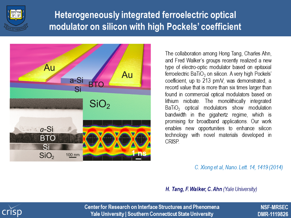
This seed project aims at transforming the novel ferroelectric materials developed by the Yale MRSEC team to practical use in silicon photonic technology. Specifically, we will develop a high speed, low power, compact electro-optical modulator based on ferroelectric barium titanite thin film epitaxially grown on silicon. The success of this project will enable the integration of an electro-optic modulator on a ubiquitous silicon platform and lead to transformative change in integrated optics.
